Huawei and SMIC made 5nm chips
Category: ICT
Published: 2025
#2519b
ChipCrunch
25822u
Title
Huawei and SMIC made 5nm chips
HuaweiとSMICは5nm半導体を製造
Index
Key
; ;
Key
Description
Remarks
>Top 0. Introduction:
0. SAQP技術:
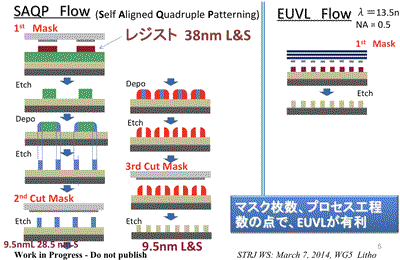
- 自己整合四重Patterning: Huawei to SICarrierの特許;
EUVを使わずDUV露光装置による微細パターン形成技術’
0. Self Aligned Quadruple Patterning (SAQP):
>Top 1. Huawei and SMIC made 5nm chips:
https://www.youtube.com/watch?v=OzAd5-pABL4 (2025/8 ChipCrunch)
- <President Trump, etc.>
“Huawei is very dangerous.” Rarely does a country go to war with a private company. “We have met the enemy and it is Huawei.” “We’re not going to do business with Huawei.” “Huawei represents a national security risk.” But is this really about Huawei or is it something bigger than that?
- 20% yield. That’s the harsh reality facing China’s most advanced semiconductor production lines right now. While the world debates whether China can truly compete in cuttingedge chip manufacturing, a stunning*3 revelation has emerged from behind the closed doors of SMIC*4’s fabrication facilities. The company that shocked the global tech industry by producing 7 nm chips for Huawei’s Mate 60 Pro*10 smartphone is now pushing into even more ambitious territory, attempting to manufacture 5 nm semiconductors without access to the West’s most critical chipmaking tools. The stakes*5 couldn’t be higher. Every smartphone is your pocket, every AI system powering the future, and every advanced military system depends on these tiny silicon wafers.
- And right now, in facilities across China, engineers are attempting what many industry experts deemed impossible just two years ago. They’re trying to produce chips that match the world best using equipment that’s fundamentally inferior to what their competitors possess. When SMIC successfully produced the Kirin 9000’s processor for Huawei’s flagship phone, it sent shock waves through Washington and Silicon Valley. Here was proof that despite America’s most stringent technology export controls, Chinese companies had found a way forward.
- But the real story goes much deeper than resilience*6. It’s about an entire nation reorganizing its industrial base around a singular goal, technological independence. The journey to this moment began when the US cut off China’s access to extreme ultraviolet lithography machines (EUV), the Crown Jewels of semiconductor manufacturing. These machines, produced exclusively by Dutch company ASML, use light wavelength of just 13.5 nm to etch impossibly small circuits onto silicon wafers. Without them, producing chips below 7nm becomes exponentially more difficult and expensive.
- Yet, SMIC pressed forward, developing what industry insiders call brute force methods to achieve similar results. Inside SMIC’s facilities, engineers have turned to multi-patterning techniques, essentially using older deep ultraviolet lithography machines (DUV). It’s like trying to paint the Moana Lisa with a house painting brush. Theoretically possible but requiring extraordinary skill and patience. The process involves exposing the same chip layer multiple times with slightly offset*15 patterns, building up the intricate*16 circuitry*17 through sheer repetition and precision. The economic implications are staggering. Industry sources reveal that SMIC’s production cost for these advanced chips run 40 to 50% higher than Taiwan’s TSMC, the world leading chip manufacturer. Even more concerning, their yields, the percentage of functional chips produced, hover below 30% of what TSMC achieves. In an industry where profit margins depend on efficiency and scale, these numbers would typically spell*19 disaster.
- Yet, Huawei and SMIC continue to push forward, driven by forces that transcend normal market economics. The Chinese government has poured billions into semiconductor development, viewing it not as a business venture, but as a matter of national security and technological sovereignty. President Xí Jìnpíng himself has made semiconductor independence a cornerstone of China’s economic strategy, declaring that the nation must master its own core technologies. The pressure intensified when Taiwan, long considered politically neutral in the semiconductor wars, took the unprecedented step of blacklisting both Huawei and SMIC. This move requires Taiwanese companies to obtain special licenses before conducting any business with these Chinese firms, effectively cutting off another potential source of advanced semiconductor technology and expertise. The decision marks a significant shift in Taiwan’s stance, reflecting the growing militarization of technology competition in the Asia-Pacific region.
- Despite these obstacles, Chinese companies are finding innovative workarounds. While industry experts remain skeptical about achieving commercially viable yields with these methods, the mere attempt represents a fundamental shift in how China approaches technological challenges. The real test comes with Huawei’s Ascend 910C*14, an AI chip that the company plans to mass-produce in early 2025. This processor designed to compete NVIDIA’s dominant AI chips, represents China’s most ambitious semiconductor project to date. Early samples have been distributed to select technology firms, but the 20% yield rate remains a critical bottleneck. Industry standards typically require yields above 70% for commercial viability, meaning Huawei must somehow triple its success rate while using inferior equipment.
- Yet, American officials are closely monitoring every development, recognizing that even partial success could reshape global technology competition. The fear in Washington isn’t just about smartphones or computers. It’s about AI, quantum computing, and military applications that depend on cuttingedge semiconductors. The transformation extends beyond just chip manufacturing. Satellite imagery recently revealed massive expansion at Huawei’s production facilities with new buildings and equipment installations suggesting preparation for large-scale manufacturing. These developments indicate that despite the technical challenges, Chinese companies are betting their future on achieving semiconductor independence. What makes this story particularly compelling is how it challenges conventional wisdom about innovation and technological progress.
- For decades, the semiconductor industry has operated on the principle that only a handful of companies with access to the most advanced equipment could produce cuttingedge chips. China’s approach using older technology in novel ways accepting higher costs and lower yields in exchange for independence represents a completely different model of technological development. The human cost of this technological marathon reveals itself in the exhausted faces of engineers working 18-hours days across China’s semiconductor facilities. One anonymous engineer from SMIC’s Shanghai plant described the atmosphere as wartime production where failure isn’t just a career setback. It’s viewed as letting down an entire nation. This pressure has created an unprecedented brain drain reversal*21. With thousands of Chinese semiconductor experts returning from Silicon Valley and Taiwan, lured by massive salaries and the promise of making history, the numbers tell a remarkable story.
- Between 2020 and 2024, over 3,500 semiconductor engineers relocated from the US to China. According to Linkedin data analysis, many site not just financial incentives with salaries often triple their American counterparts, but a sense of participating in something bigger than quarterly earnings reports. This mass mobilization extends to China’s education system where semiconductor engineering programs have expanded by 400% since 2019. Universities in Beijing, Shanghai, and Shēnzhèn have created specialized tracks that fastback students into the industry with guaranteed employment and housing subsidies. The Chinese Academy of Sciences launched Project Chip Pioneer, aiming produce 100,000 qualified semiconductor engineers by 2030, a number that would dwarf*23 the combined workforce of TSMC and Samsung.
- Yet, the technical challenges remain monumental. SMIC’s attempts at 5 nm production using DUV require what experts call quadruple patterning. Exposing each layer four times with microscopic precision. The margin for error shrinks to atomic levels where a misalignment of just 2 nm can render an entire wafer worthless. The economic toll continues mounting. Conservative estimates suggest China has invested over 150 billion in semiconductor development since 2014, with another 300 billion committed through 2030. These figures dwarf the chips acts 52 billion allocation in the US though American spending benefits from existing infrastructure and expertise. The question haunting Beijing’s policymakers. Can money alone overcome technological barriers that took decades to develop?
- International reactions have been mixed but revealing. Japan recently tightened its own export controls on 23 types of semiconductor manufacturing equipment, closing potential loopholes China might exploit. South Korea faces a more complex dilemma with Samsung and SK Hynix operating major facilities in China that produce 40% of their NAND flash memory. These companies must navigate between American pressure and Chinese market realities, walking a tight rope that grows thinner each month. The ripple effects touch unexpected corners of the global economy.
- Rare earth prices surged 30% in 2024 as China restricted exports of Ga and Ge, essential materials for semiconductor production. This resource nationalism represents Beijing’s counterpunch to Western technology restrictions, weaponizing its dominance in critical materials. Behind closed doors, even American officials acknowledge China’s progress has exceeded worst case scenarios from
just 3 years ago. A classified Pentagon assessment partially leaked to Reuters suggests Chinese military systems could achieve semiconductor parody in specialized applications by 2027. Coincidentally, the date President Xi identified for military readiness regarding Taiwan, this timeline has accelerated American efforts to strengthen alliance with Japan, South Korea and the Netherlands, creating what some call a semiconductor NATO.
- The human stories emerging from this technological Cold War paint a complex picture. Leume, a 28-year-old process engineer at SMIC, hasn’t taken a day off in 6 months. Her team recently achieved a breakthrough reducing defect rates by 12% of victory celebrated with tears and champagne at 3:00 am in the FAB facility. Yet, skeptics remain vocal. Bob Davis, former VP at Applied Materials, argues that China’s approach fundamentally misunderstands semiconductor economics.
1. :
- <Trump大統領ほか> "Huaweiは非常に危険だ"
"我々私たちは敵に会った、それはHuaweiだ"
"我々はHuaweiとビジネスをするつもりはない” "Huaweiは国家安全保障上のリスクがある"
これらの一連の発言のように一国が民間企業と戦うことは極めて」稀なことです。しかしこれらは本当にhuaweiに対してなのでしょうか、それともそれよりも大きなものに対してなのでしょうか?
- 歩留まりは20%。それは、現在中国が、最も高度な半導体生産ラインに直面している厳しい現実です。世界は、中国が最先端のチップ製造で真に競争できるかどうかを議論していますが、中国のfoundryであるSMICの製造施設のドアの向こうから驚くべき発表がありました。 Huaweiのスマホ用のMate60 Proという7 nmのチップを生産することで世界のハイテク産業に衝撃を与えた会社は、さらに西側のチップ製造装置に依存せずに5 nmの半導体を製造しようとする野心的な計画を明らかにしたのです。これ以上の大きな賭け事はありません。それはポケットに入るすべてのスマートフォン用であり、未来に関わるすべてのAIシステム用であり、すべての高度な軍事システムもこれらのの小さなシリコンチップに依存しているのです。
- そして今、中国の至る所の施設では、エンジニアは2年前には、多くの業界の専門家が不可能と見なしてたことに挑戦しています。彼らは、競合他社が持っているものより基本的に劣っている機器を使用して、世界に競合するチップを生産しているのです。 SMICがHuaweiの主要な」携帯電話用のKirin 9000のプロセッサを成功裏に作成したとき、ワシントンとシリコンバレーに衝撃波が伝わりました。ここでは、米国で最も厳しい技術輸出管理にもかかわらず、中国企業が今後解決策を見つけたという証拠になりました。
- しかし、実際の話はそのショックよりもはるかに深いのです。それは、国全体が総力を挙げて、単一の目標、技術の独立性を中心に、産業基盤を再編成する姿勢でいることです。この方向への転換は、米国が中国が半導体製造の王冠の宝石である超紫外線リソグラフィ (EUV)の輸出禁止したときに始まりました。オランダの会社ASMLのみが生産するこれらのEUVは、わずか13.5 nmの光波長を使用して、シリコンウェーハに信じられないほど小さな回路を露光します。それらがなければ、7nm以下のチップを製造することは、指数関数的により困難でかつ高価になります。
- しかし、SMICは技術革新し、業界関係者が同様の結果を達成するために力づくの方法と呼ぶやり方で開発しました。 SMICの施設内では、エンジニアは基本的に古い深紫外線リソグラフィ(DUV)を使用して、多重露光の方法に目を向けています。それは、いわば家庭にある普通の絵筆でモアナ・リザを描写しようとするようなものです。理論的には可能ですが、並外れたスキルと忍耐が必要です。このプロセスでは、同じチップ層をわずかにオフセットしたパターンで複数回露出し、複雑な回路を繰り返しの精度で描画することが含まれます。その経済的影響は驚異的です。業界の情報筋は、これらの高度なチップのSMICの生産コストは、世界をリードするチップメーカーである台湾のTSMCよりも生産コストが40〜50%高くなっていると推定しています。さらに、彼らの歩留まりである製造されたチップの割合は、TSMCが達成したものの30%以下であろうとしています。利益率が効率と規模を重視している業界としては、これらの数値は通常は大きな損失を伴います。
- しかし、HuaweiとSMICは、通常の市場経済を超越する力によって推進されており、前進し続けています。中国政府は、数十億ドルを半導体開発に注ぎ込んでおり、それをビジネスベンチャーとしてではなく、国家安全保障と技術的主権の課題と見なしています。 習近平主席自身が半導体の独立性を中国の経済戦略の基礎とし、国が独自のコアテクノロジーを習得しなければならないと宣言しました。半導体戦争では、長い間政治的に中立だと考えられていた台湾が、HuaweiとSMICの両方をブラックリストに登録するという前例のない手続きを踏んだとき、圧力が強まりました。この動きでは、台湾企業がこれらの中国企業とのビジネスを行う前に特別なライセンスを取得する必要があり、高度な半導体技術と専門知識の拡散を効果的に遮断しています。この決定は、アジア太平洋地域での軍事技術競争の激化を反映して、台湾の姿勢に大きな変化を与えています。
- これらの障害にもかかわらず、中国企業は革新的な回避策を見つけています。業界の専門家は、これらの方法で商業的に有効な歩留まりを達成することに懐疑的ですが、中国が技術的課題にどのように挑戦するかのついて注視しています。実際の製造としては、2025年初頭に大量生産する予定のAIチップである HuaweiのAscend 910Cに注目しています。このプロセッサは、NVIDIAの支配的なAIチップに競うように設計されており、中国で最も野心的な半導体プロジェクトでもあります。初期の試作品は、一部のテクノロジー企業に配布されていますが、20%の歩留まり率は依然として重要なボトルネックです。業界の基準では、通常、商業的実行可能な採算のためには歩留まり率は70%を超える比率が必要です。つまり、Huaweiは劣等な機器を使用しながら歩留まり率を何らかの形で3倍にしなければならないのです。
- しかし、米国の当局はすべての開発を綿密に監視しており、部分的な成功でさえグローバルな技術競争を再考しなければならないとしています。ワシントンにとっての脅威は、スマートフォンやコンピューターだけではありません。 AI、量子コンピューティング、および最先端の半導体に依存する軍事用途に関するものです。その変化は、チップ製造を超えて大きく拡張されます。最近のGPS画像では、Huaweiは、大規模な製造の準備を示す新しい建物と機器の設置を備えた生産施設での大規模な拡張を明らかにしました。これらの開発は、技術的な課題にもかかわらず、中国企業が半導体の独立性を達成することに将来を賭けていることを示しています。この動向が注目に値するのは、イノベーションと技術の進歩を目指して従来の知恵に対してどのように挑戦していくのかについてです。
- 何十年もの間、半導体業界は、最も高度な機器にアクセスできる少数の企業のみが最先端チップを製造できるという原則で運営されてきました。古い技術を斬新な方法で活用するという中国のアプローチは、高いコストとより低い歩留まり率を受け入れることでチップ生産の独立を目指そうというものです。これは、技術開発のまったく異なるモデルでもあります。この技術マラソンの人的コストは、中国の半導体施設全体で18時間も働くエンジニアの疲れ果てた顔に現れています。 SMICの上海工場のエンジニア(匿名)によれば、戦時の生産工場のようであり、失敗は単なる個人の評価にとどまらないと説明しています。国全体を失望させることになると見なされているからです。この圧力により、前例のない頭脳流出の逆転現象が生じました。シリコンバレーと台湾から何千人もの半導体の専門家が中国大陸に戻ってきて、高額な給料と歴史的な役割への参加に誘われており、関与する人材は驚くべき数字に達しています。
- 2020年から2024年の間に、3,500人以上の半導体エンジニアが米国から中国に帰国しました。 LinkedInのデータ分析によると、給与を伴う金銭的待遇だけでなく、多くの場合、アメリカの同業者の3倍に達するだけでなく、四半期ごとの収益よりも大きな役割に参加しているという実感が報告されています。この大規模な動員は、2019年以降、中国の教育システムでは、半導体エンジニア養成計画が4倍にも拡大しているにまでなっています。中国科学アカデミーではチップパイオニアプロジェクトを立ち上げ、2030年までに100,000人の半導体エンジニア有資格者を養成しました。この数はTSMCとSamsungの労働力を合わせた数を凌駕しています。
- しかし、技術的な挑戦はまだ記念碑的なままです。 DUVを使用した5 nmの製造でのSMICの試みは、顕微鏡を使用しての四重層パターンと呼ぶものが必要です。各層を顕微鏡的な精度で4回露出させます。エラーの余地は、原子レベルであるわずか2 nmの不具合しか許されず、配線に失敗すると、ウェーハ全体を無駄になります。経済的費用は引き続き増加しています。保守的に推定しても、中国は2014年以来、半導体開発に1500億ドルを超える投資を行っており、さらに2030年までに3000億ドルを投資しようとしています。これらの数字は、既存のインフラと専門家を擁しているとはいえ、米国がチップ生産に投じている520億ドルの費用に比べて圧倒的に多額になっています。北京の政策立案者を悩ませる質問としては、費用をかけえて、数十年間発展させれば、技術上の障壁を克服できるのかという課題なのです。
- 国際的な反応は様々ですが、明らかになってきていることがあります。日本は最近、23種類の半導体製造装置に関する独自の輸出管理を厳格にし、中国が利用する可能性のある潜在的な抜け穴を封じました。韓国は、より複雑な状況に直面しており、SamsungおよびSK Hynixは、NANDフラッシュメモリの40%を生産する中国の主要施設を運営しています。これらの企業は、アメリカの圧力と中国の市場という現実の間で工夫しながら、毎月厳しく狭いロープ上を歩いています。波及効果は、世界経済の予期しない方向に現れてきます。
- 2024年にレアメタルの価格は30%も急騰しました。これは中国が半導体生産に不可欠な材料であるGaとGeの輸出を制限したためです。この資源」ナショナリズムは、西洋の技術制限に対する北京の対抗措置を表しており、重要な資源におけるその優位性を兵器化しています。アメリカ当局でさえ、3年前に比べて中国のこの政策の進展が最悪のシナリオを超えていることを認めています。ロイターに部分的入手した米国国防総省の秘密報告では、2027年までに中国の軍事システムが、半導体技術の模倣により専門的なアプリケーションを開発できることを示しています。偶然にも、習近平主席は台湾に関する軍事的な準備を特定し、このタイムラインは日本、韓国、オランダの同盟関係を強化して、いわば半導体生産のNATO版を構築すべく米国の努力を加速しました。
- この技術的な冷戦から生じたストーリーは、複雑な展開の絵を描きます。 SMICの28歳のプロセスエンジニアであるLeume氏は、6か月も休暇を取っていません。彼女のチームは最近、製品の欠陥率を12%も改善した勝利を祝って、工場施設内で午前3時に涙とシャンパンで乾杯したとのことです。。しかし、懐疑論者は声を上げています。 Applied Materialsの元VPであるBob Davisは、中国のアプローチは半導体経済学を根本的に誤解しているのではと主張しています。
- a
- foundry: 半導体受託製造専門会社
- stunning: 衝撃的な
- SMIC: 中芯国際集成電路製造有限公司)
- stake: 掛け金; 競争
- resilience: ショックからの回復力
- Huawei Mate 40Pro: Kirin 9000搭載(5nm chip) TDP, thermal design power; 6W
- transcend: 超越する
- workaround: program /systemの問題の一時的な解決
- Ascend 910C: SMIC 第二世代 7nm process (N+2)で製造。HuaweiのSWに合わせてHWを最適化。Da Vinci architectureを採用。530億個transistorを統合。消費電力300W; NVIDIAのH100に匹敵? (2025/5): Ascend 920を2025下期から量産開始と発表 (SMIC 6nm process node)
Cf: NVIDIA H100, H200とAMDのMI300X
Cf: 2024 1Q Foundry順位:
1) TSMC 62%,
2) Samsung 13%, 3) SMIC 6%,
4) 台UMC 6%,
5) 米Global Foundries 5%,
6) 中Huahong 2%
- offset: ずらした >SAQP tech
- intricate: 複雑な
- circuitry: 電気回路構成
- imagery: 画像, 映像
- spell: 好ましくない結果をもたらす; 〜 trouble
- a
- brain drain reversal: 頭脳流出の反転
- a
- dwarf: cause to seem small
- a
- render: provide or give
- revealing: 明らかにする
- a
>Top2. Huawei's 6G revolution:
https://www.youtube.com/watch?v=E8CeWTDo-DQ
- No Western Approval, No Problem: Inside Huawei’s 6G Revolution: Imagine waking. Imagine for a mom that you’re watching a remote surgery unfold in real time. Except the patient is on another continent and you can see every blood vessel, every subtle tremor*3 in perfect 3D. There’s no lag, no buffering, just seamless, instantaneous interaction. It sounds like science fiction, yet it’s precisely the kind of feat*5 6G promises to deliver. But while most of us are still marveling at what 5G has brought, there’s a high-stakes*5 race underway that could completely redraw the map of global connectivity.
- And Huawei is at its very heart. Back when 5G was just becoming a household*6 name, Huawei quietly shifted its gaze to the next frontier. Even as Western regulators barred*7 the company from key markets, citing security concerns and effectively trying to choke off*8 its growth, Huawei double down*9 on research. By 2017, while before most telecom giants even had their 5G strategy in place, the company was already funneling*11 huge resource into theoretical 6G models. And by late 2020, long before the world had finished installing 5G infrastructure, China launched its first experimental 6G satellite, sending terahertz signals from orbit to test the feasibility of speeds 100 times faster than anything we’ve seen so far.
- To appreciate why this matters, consider the challenges that shape the 5G era. Rolling out faster networks was as much a political saga* as it was a technological one. Governments wielded*13 approvals like swords and without access to Western allies supply chains. Many companies found themselves boxed out*14. Huawei, despite its engineering prowess*15, faced bans in Europe, North America, and parts of Asia, all in the name of national security. Many analysts concluded that no amount of innovation could overcome the lack of Western endorsement. Yet, Huawei’s response wasn’t retreat. It was a pivot to self-reliance, a move that now looks like a master stroke.
- What makes 6G fundamentally different isn’t just raw speed. We’re talking terabit per second data rates, end-to-end latency measured in microseconds, and networks so smart they can reconfigure themselves in real time. Picture a fully immersive augmented reality concert attended by millions. Each audience member seeing the event from a unique angle or an autonomous drone fleet coordinating disaster relief without a single dropped packet. These are’t far-off dreams. They’re the very use cases driving today’s 6G prototypes. Yet, the real lynch pin*16 of this future is advanced semiconductors. For years, the most cuttingedge chips have depended on EUV lithography machines. Tools so complex and so controlled that only a handful of Western companies can produce them.
- China’s foundries were effectively cut off from these machines by export controls, leading many to believe that without EUV, Chinese chipmakers would remain stuck several generations behind. But you might not know is that China’s leading semiconductor foundry SMIC has quietly performed a 2nm gate all-around transistor process using only deep ultraviolet (DUV) lithography. This breakthrough shatters the assumption that EUV is the only path to the most advanced nodes. The implications of this are staggering. If SMIC can produce chips at the bleeding edge*17 without EUV, then Huawei, SMIC’s largest customer, can design and deploy processors powerful enough to drive AI native 6G networks, all without Western approval or supply chain access.
- Overnight, the strategic leverage that Western nations thought they has evaporated*18. Suddenly, the narrative shifts from Huawei is at the mercy of*19 export controls to Huawei has unlocked an independent route to the future. Still, innovation on paper doesn’t always translate to real world impact. That why Huawei’s research goes far beyond theoretical white papers. Inside their R&D centers in Shēnzhèn, teams of engineers and data scientists run thousands of networks simulations daily. They’re not just testing throughput, they’re steps testing entire ecosystems. Everything from self-healing cell towers that reroute traffic around power failures to intelligent-based stations that predict peak demand periods and preemptively*20 adjust resource allocations. These aren’t incremental tweaks*21. They’re a wholesale rethinking of how wireless networks operate.
- At the same time, Huawei has been forging alliances with academic institutions and national labs across China. Their partners are developing integrated sensing and communication modules that allow every 6G device to double as an environmental sensor. Imagine your smartphone picking up subtle vibrations in a nearby bridge, alerting civil engineers to structural fatigue long before any cracks appear. It’s a fusion of IoT, big data, and AI that promises to build a digital twin of our physical world. One that’s updated in real time and accessible from anywhere. But the breakthroughs of this scale always come with risks.
- When networks become that intelligent, when they can anticipate your movements, predict your needs, and even infer your emotional state, the potential for privacy abuse balloons. It’s easy to imagine a future where every interaction is logged. Every preference tracked, and every personal decision influenced by unseen algorithms. Huawei’s vision for an AI native network raises questions about where data sovereignty ends and surveillance begins. Even more, if two incompatible 6G ecosystems emerge, one governed by Western data privacy norms, the other by China’s state-driven model. Global interoperability could fracture, leaving billions of devices stranded*22 in the digital no man’s land between them.
- Economically, the stakes couldn’t be higher. Industry forecasts estimate that the value of the 6G enabled market, covering everything from autonomous vehicles to immersive tele-sence, could top 13 trillion by 2035. If Huawei’s independent 6G strategy succeeds, it stands to capture a significant share of that market. Conversely, Western companies may need to scramble to build new fabs, secure domestic supply chains, and rewrite their technology playbooks.
- Europe and the US have already announce plans to pour tens of billions into local chip manufacturing. What seemed like forward-thinking industrial policy now feels like a desperate response to a strategic surprise. Even more intriguing*23 is what this means for the geopolitical landscape. Fore decades, technological standards have been a form of soft power. Whoever sets the rules for cellular networks from GSM in the 1990s to 5G today wins influence in global market, in global trade negotiations, and ultimately in global politics. If China and Huawei can cement their own 6G framework, complete with homegrown chipsets, proprietary AI optimizations and a nationalized data governance model, they’ll effectively create a parallel digital sphere.
- Countries aligning with that sphere might gain access to advanced infrastructure at lower cost, but at the expense of deeper integration with Western-led ecosystems. It’s a strategic gamble that could redraw the map of alliances in everything from digital trade to military communications. Of course, Western governments aren’t sitting still. In parallel with funding new fabs, they’re doubling down on open-source network initiatives and pushing for more stringent data privacy safeguards 6G standards bodies.
- The battle for the International Telecommunication Union’s working groups has already intensified with each side lobbying for language that favors their architecture. Ai native versus cloud native centralized orchestration versus distributed edge first processing. The standard documents may read like dry legal ease, but the outcome will dictate which companies win contracts for smart cities, autonomous logistics, and next generation mobile broadband. Amid all this, Huawei’s public messaging has been remarkable consistent. Innovation under pressure, they call it. The company has released periodic white papers outlining their vision for a secure AI-driven network that balances performance with resilience.
- Yet for all their optimism, few outside China have seen the full scale of their prototype deployments. That begins to change this year as Huawei plans limited commercial trials in partner cities in Asia and Africa, where regulatory barriers are lower and demand for connectivity solutions is sky-high. These field trials will test not just speed and latency, but real world use cases, emergency response coordination, remote manufacturing supervision, and large-scale environmental monitoring. Perhaps the most compelling glimpse of what’s coming can be seen in a recent demonstration in Guǎngzhōu. There, Huawei engineers showcased a live holographic collaboration between sweet level cameras, autonomous vehicles, and a remote control center hundreds of miles away. The entire loop from sensing to inference to actuation completed in under 50 μs. It wasn’t just a flashy demo. It was proof that terahertz links and Ai orchestration can sync up multiple network layers in real time.
- And critically, all the processing happened on chips manufactured in China using DUV lithography, sides stepping any Western technology blockade. Still, fore viewers and decision makers watching from afar, the unanswered questions remains. Will this Chinese-led 6G ecosystem be an isolated island, or will it merge back into a global network tapestry? Some experts argue that economic incentives will eventually force compatibility, just as 3G and 4G systems converge despite early fragmentation. Others warn that the sheer*26 complexity of AI native architectures combined with divergent security protocols could make seamless integration impossible. In either scenario, the notion of a single universally accessible network is fading.
2. Huaweiの6G通信革命:
- 欧米の承認なしでも問題なし:Huaweiの6G革命です。例えば、目覚めたときに、母親が遠隔手術を受けている様子をリアルタイムで見ているところを想像してみてください。ただし、患者は、別の大陸にいて、すべての血管、あらゆる微妙な震えまでも完璧な3Dで見ることができるのです。遅延も緩衝もなく、シームレスで瞬時のやり取りが実現します。まるでSFのように聞こえますが、まさに6Gが約束する離れ業*4なのです。しかし、私達の多くが5Gのもたらした成果にまだ驚嘆している一方で、世界の接続地図を完全に塗り替える可能性のある熾烈な競争が繰り広げられています。
- そして、その中心にはHuaweiがいます。5Gがようやく一般に知られるようになった頃、Huaweiは静かに視線を次のフロンティアへと移しました。欧米の規制当局が安全保障上の懸念を理由に同社を主要市場から締め出し、事実上同社の成長を阻止しようとした中で、Huaweiは研究にさらに力を入れたのです。2017年に、ほとんどの通信大手が5G戦略を策定する前、同社はすでに理論上の6Gモデルに膨大なリソースを投入していました。そして2020年末、世界が5Gインフラの設置を終えるずっと前、中国は初の実験用6G衛星を打ち上げ、軌道からtera Hz信号を送信し、これまでよりも100倍も速い速度の実現可能性をテストしました。
- これがなぜ重要なのかを理解するには、5G時代を形作る課題を考えてみましょう。より高速なネットワークの展開は、技術的な課題であると同時に、政治的な課題でもありました。各国政府は承認をまるで剣のように振り回し、西側諸国の同盟国のサプライチェーンへのアクセスも遮断しました。多くの企業は締め出されました。Huaweiは、その優れたエンジニアリング力にもかかわらず、欧州、北米、そしてアジアの一部で国家安全保障の名の下の禁止措置に直面しました。多くのアナリストは、どんなに革新的であろうと、西側諸国の支持の欠如を克服することはできないと結論づけました。しかし、Huaweiの対応はそれで後退することはありませんでした。それは自立への転換であり、今となっては賢明な方針とも言える動きでした。
- 6Gを根本的に異なるものにしているのは、単なる速度ではありません。tera bit/sのデータレート、μ秒単位で測定されるエンドツーエンドの遅延、そしてリアルタイムで自己再構成できるほどスマートなネットワークです。数百万人が参加する、没頭した拡張現実コンサートを想像して見て下さい。観客一人ひとりが独自の角度からイベントを鑑賞したり、自律型ドローンが災害救助活動を調整し、パケットの欠落を一切起こさない様子を想像して見て下さい。これらは遠い夢ではありません。まさに今日の6Gプロトタイプの代表的な使用実例です。しかし、この未来の真の要となるのは、高度な半導体です。長年にわたり、最先端のチップはEUVリソグラフィー装置に依存してきました。この装置は非常に複雑で高度に制御されているため、欧米のほんの一握りの企業しか製造できないのです。
- 中国のファウンドリーは輸出規制によってこれらの製造機器から事実上遮断されており、EUVがなければ中国のチップメーカーは数世代遅れを使い続けるだろうと多くの人が考えていました。しかし、中国の大手半導体ファウンドリーであるSMICが、深紫外線(DUV)リソグラフィーのみを使用した2nmゲートオールラウンドトランジスタプロセスを背後で着々と実行していたことはあまり知られていません。この画期的な進歩は、EUVが最先端ノードへの唯一の道であるという前提を打ち砕きます。その意味合いは計り知れません。SMICがEUVなしで最先端のチップを製造できるのであれば、SMICの最大の顧客であるHuaweiは、AIネイティブ6Gネットワークを稼働させるのに十分強力なプロセッサを設計・開発することができ、しかも西側諸国の承認やサプライチェーンへのアクセスは必要なくなるのです。
- 西側諸国が考えていた戦略的影響力は、一夜にして霧消してしまったのです。突如、Huaweiは輸出規制に翻弄されているという見方から、Huaweiが未来への独自の道を切り開いたという見方へと変化しました。しかし、机上だけの空論的なイノベーションでは必ずしも現実世界への影響につながるわけではありません。だからこそ、Huaweiの研究は理論上のレポートでの研究をはるかに超えているのです。深圳のR&Dセンターでは、エンジニアとデータサイエンティストのチームが毎日何千ものネットワークシミュレーションを実行しており、単にスループットをテストしているのではなく、エコシステム全体を段階的にテストしているのです。停電時にトラフィックを再ルーティングできる自己修復型のセルタワーから、ピーク需要期間を予測し、事前にリソース割り当てを調整するインテリジェントベースのステーションまで、あらゆるものが対象となります。これらは、段階的な微調整ではなく、無線ネットワークの運用方法を根本から見直すものです。
- 同時に、Huaweiは中国全土の学術機関や国立研究所と提携関係を築いてきました。パートナー企業は、あらゆる6Gデバイスを環境センサーとしても機能させる統合型センシング・通信モジュールを開発しています。スマートフォンが近くの橋の微妙な振動を感知し、亀裂が生じるかなり前に土木技術者に構造疲労を警告する様子を想像して見て下さい。これはIoT、ビッグデータ、AIを融合させたもので、現実世界のデジタルツインを構築することを意味しています。リアルタイムで更新され、どこからでもアクセスできるデジタルツインです。しかし、このような規模のブレークスルーには常にリスクが伴います。
- ネットワークがこれほどインテリジェントになり、ユーザーの動きやニーズを予測し、さらには感情状態まで推測できるようになると、プライバシー侵害の可能性は膨れ上がります。あらゆるやり取りが記録される未来を想像するのは容易になります。あらゆる嗜好が追跡され、個人の様々な意思決定が目に見えないアルゴリズムによって左右されるのです。HuaweiのAIネイティブネットワーク構想は、データ主権はどこで終わり、監視はどこで始まるのかという疑問を提起しています。さらに、もし互換性のない2つの6Gエコシステムが出現し、一方が欧米のデータプライバシー規範に、もう一方が中国の国家主導モデルに支配されるような事態になれば、世界的な相互運用性が崩壊し、数十億ものデバイスが両者の間のデジタル無人地帯に取り残される可能性がでてきます。
- 経済的には、この状況はこれ以上ないほど深刻です。業界予測によると、自動運転車から没入型テレセンスまで、あらゆるものをカバーする6G対応市場の価値は、2035年までに13兆ドルを超えると見込まれています。Huaweiの独自の6G戦略が成功すれば、同社はこの市場の大きなシェアを獲得することになるでしょう。一方、欧米企業は、新たな工場の建設、国内サプライチェーンの確保、そして技術戦略の見直しを急ぐ必要が出てきます。
- 欧州と米国はすでに、数百億ドル規模の現地半導体製造への投資計画を発表しています。先進的な産業政策と思われていたものが、今や戦略的なサプライズへの必死の対応のように思えます。さらに興味深いのは3、これが地政学的状況にどのような影響を与えるかということです。数十年にわたり、技術標準は一種のソフトパワーでした。1990年代のGSMから今日の5Gに至るまで、携帯電話ネットワークのルールを策定する者は、世界市場、世界貿易交渉、そして最終的には世界政治において影響力を獲得するのです。中国とHuaweiが、国産チップセット、独自のAI最適化、国営データガバナンスモデルを備えた独自の6Gフレームワークを構築できれば、実質的に並行するデジタル領域を構築できることになります。
- この領域に足並みを揃える国々は、先進的なインフラをより低コストで利用できる可能性がありますが、西側主導のエコシステムとのより深い統合を犠牲にすることにもなります。これは、デジタル貿易から軍事通信に至るまで、あらゆる分野で同盟関係の構図を塗り替える可能性のある戦略的な賭けです。もちろん、西側諸国政府は手をこまねいているわけではありません。新たなファブへの資金提供と並行して、オープンソースネットワークへの取り組みを強化し、6G標準化団体に対し、より厳格なデータプライバシー保護の導入を強く求めています。
- 国際電気通信連合 (ITU) の作業部会をめぐる争いはすでに激化しており、それぞれの陣営は自国のアーキテクチャに有利な文言を求めてロビー活動を行っています。AIネイティブ vs. クラウドネイティブ 集中型オーケストレーション vs. 分散型エッジファースト処理。標準化文書は一見、味気ない法的緩和策のように聞こえるかもしれませんが、その結果は、スマートシティ、自律物流、次世代モバイルブロードバンドといった分野の契約獲得において企業の命運を左右することになります。こうした状況下において、Huaweiの広報メッセージは驚くほど一貫しています。彼らはこれを"プレッシャーの下でのイノベーション"と呼んでいます。同社は、パフォーマンスと回復力のバランスが取れた安全な AI 駆動型ネットワークのビジョンを概説したホワイト ペーパーを定期的に公開しています。
- しかし、こうした楽観的な見通しにもかかわらず、中国以外でプロトタイプの本格的な展開を目にした人はほとんどいません。しかし、今年、Huaweiは規制障壁が低く、接続ソリューションの需要が非常に高いアジアとアフリカのパートナー都市で限定的な商用実証実験を計画しており、状況は変わり始めています。これらのフィールドトライアルでは、速度と遅延だけでなく、実際の使用経験、緊急対応の調整、遠隔製造監視、大規模な環境モニタリングなどもテストされます。今後の展開を最も印象深く垣間見ることができるのは、広州で最近行われたデモンストレーションでしょう。Huaweiのエンジニアたちは、スイートレベルカメラ、自律走行車、そして数百マイル離れた遠隔制御センターとの間で、ホログラフィックなライブコラボレーションを実現しました。センシングから推論、そしてアクチュエーションまでの全ループは50μs未満で完了しました。これは単なる派手なデモではありませんでした。Tera HzとAIオーケストレーションによって、複数のネットワークレイヤーをリアルタイムで同期できることを実証したのです。
- そして重要なのは、すべての処理がDUVリソグラフィーを使用して中国で製造されたチップ上で行われ、西側諸国の技術封鎖を回避していることです。それでも、遠くから見守る視聴者や意思決定者にとっては、未解決の疑問が残ります。この中国主導の6Gエコシステムは孤立した島になるのか、それともグローバルネットワークの統合環境に再び統合されるのでしょうか。一部の専門家は、3Gと4Gシステムが初期の断片化にもかかわらず収束したように、経済的インセンティブが最終的に互換性を強制することになると主張しています。他の専門家は、AIネイティブアーキテクチャの複雑さと分散したセキュリティプロトコルの組み合わせにより、シームレスな統合が不可能になる可能性もあると警告しています。どちらのシナリオでも、単一のユニバーサルアクセス可能なネットワークという概念は消滅しつつあります。
- a
- a
- subtle tremor: 微妙な震え
- feat: 妙技, 離れ業
- high stakes: 一か八かの
- household: 日常よく知られた
- bar: 参加することを禁止する
- choke off: 経済成長などを抑制する
- double down: strengthen one’s commitment to a particular strategy
- a
- funnel: 資金などをじょうごを通すように注ぐ, 進める
- saga: 込み入った長話
- wield: 影響力を振るう
- box out: rebound争いで優位に立つために、相手選手とbasketの間に立ち、相手を内側に入らせないようにすること; (例文) 多くの企業が排除されてしまった。
- prowess: 卓越した技量
- lynch pin; linch pin: 組織の中心人物
- bleeding edge: 最先端
- evaporate: 希望が徐々に消える
- at the mercy of: …の言いなりになって
- preemptively: 機先を先して
- tweak: twist or pull sharply; improve by fine adjustments
- strand: 立ち往生する
- intrigue: 興味をそそる
- sidestep: 問題を回避する
- a
- sheer: すさましい, とてつもない
>Top3. xxxx:
3. xxxx:
>Top4. xxxx<E>:
4. xxxx:
Comment
- Historically it seems inevitable that the following countries will first imitate the advanced technogies of the West, and then improve and surpass them, as was the case with Japan in 1970s and 80s.
- The spead of knowledge and improvement of knowledge mean that any constraints or restrictions will eventually be overcome.
- The key is how the followers can maintain their passion to catch up and surpass the values of the advanced technologies. Indeed, economic blockades and attempts of decoupling may actually inflame that passion.
- The extraordina efforts by the US to exclude China are a typical example to these cases.
- かつての1970-80年代日本がそうだったように、西欧による先進技術事例を最初は模倣しつつも、いずれそれを改善・凌駕してそれを追い抜くのは歴史の必然に思える。
- 知識の伝搬と改善は、どのような規制もいずれは破られる。
- 重要なのは、それを破るだけの価値と努力を後から追いかける者が、その情熱を維持できるかどうかだ。経済封鎖や関係断絶は、むしろその情熱に火をつけることになりかねない。
- 米国による異常なまでの中国排除の動きは正にこの典型的な事例と言えよう。
Huawei and SMIC made 5nm chips |
Category: ICT |
|
ChipCrunch |
25822u |
Title |
Huawei and SMIC made 5nm chips |
HuaweiとSMICは5nm半導体を製造 |
|---|---|---|
Index |
||
Key |
; ; | |
Key |
Description |
Remarks |
>Top 0. Introduction: |
0. SAQP技術:
|
0. Self Aligned Quadruple Patterning (SAQP):
|
>Top 1. Huawei and SMIC made 5nm chips:https://www.youtube.com/watch?v=OzAd5-pABL4 (2025/8 ChipCrunch)
|
1. :
|
|
>Top2. Huawei's 6G revolution:https://www.youtube.com/watch?v=E8CeWTDo-DQ
|
2. Huaweiの6G通信革命:
|
|
>Top3. xxxx: |
3. xxxx: |
>Top4. xxxx<E>: |
4. xxxx: |
Comment |
|
|